如何用PSoC UDB实现硬件PDM
0赞如何用PSoC UDB实现硬件PDM
- 基于累加的PDM算法(4)
除了FPGA/CPLD外,目前能在MCU内部实现基于累加的PDM算法的硬件PDM还只有Cypress PSoC的UDB(PSoC3-5,而PSoC1不带UDB)。本节具体介绍如何用PSoC的UDB Datapath来做基于累加算法的硬件PDM。同时这对熟悉UDB中的Datapath也有好处,因为我觉得UDB的Datapath是一项很有利用价值的资源。
开发环境为Cypress PSoC Creator 2.2,实例在最近大家都感兴趣的PSoC4上实现。
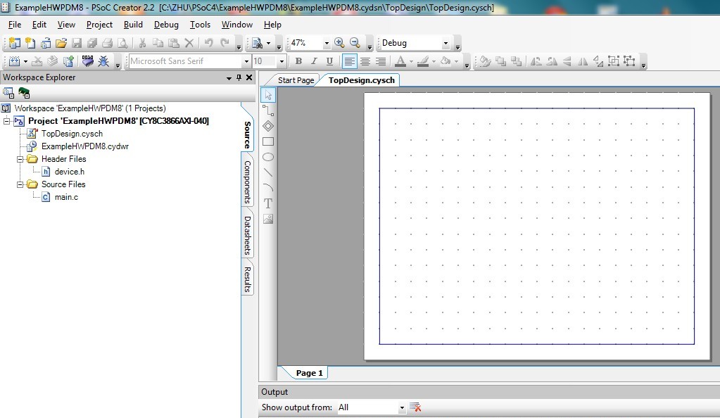
图0
我们用 File – New – Project – Empty PSoC4(CY8C42*) Design 建立项目ExampleHWPDM8后(图0),由于我们还没有PDM这个部件(Component),所以还无法画出电路图。因此必须先建立PDM这个部件,步骤如下。
(1)点垂直方向的“Components”TAB,然后右键点Project ‘ExampleHWPDM8’,选择“Add Component Item”(图1)。

图1
(2)在弹出的“Add Component Item”窗口,选择“Symbol Wizard”,并在Component Name处填上部件名称(例如)“MyPDM8B”。然后点“Create New”。(图2)
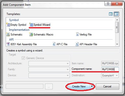
图2
(3)在弹出的“Symbol Creation Wizard”窗口,填写部件的输入、输出端。
这里输入端为clock – Digital Input。输出端为极性相反的两个输出PDM_p、PDM_n – Digital Output。“Symbol Creation Wizard”窗口会自动生成部件的电路符号。点击“OK”完成此步操作。(图3A)
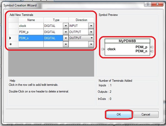
图3A
于是项目就有了可供调用的部件“MyPDM8B”的电路符号,其通用名称为“MyPDM8B_N”。将来多个同样的部件可用MyPDM8B_1、MyPDM8B_2、MyPDM8B_3区分。(图3B)
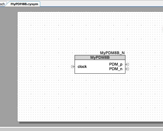
图3B
(4)点“MyPDM8B_N”图纸的空白处(右键),并选择“Generate Verilog” (图4),在弹出窗口中点击“Generate”,自动生成Verilog文件“MyPDM8B.v”。
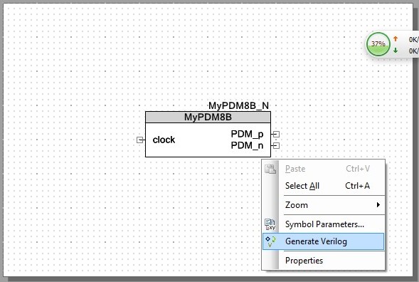
图4
(5)开发环境的主窗口自动显示Verilog文件“MyPDM8B.v”的内容,待编辑(图5A)。新生成的MyPDM8B.v未被保存,要先保存。

图5A
编辑的第一步使用Cypress PSoC Creator 2.2 开发环境提供的Datapath Config Tool完成部件“MyPDM8B”的内部结构配置。
在开发环境左边窗口用右键点文件“MyPDM8B.v”,在弹出的小窗口选“Datapath Config Tool…”(图5B)。
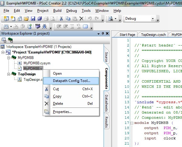
图5B
(6)自动转到Datapath Config Tool环境。
根据前面文章的介绍,我们的算法只使用“A0 = A0 + D0”一条指令,所以填写表格非常方便。
(6A)Edit – New Datapath…
本例为8位PDM,所以取Instance Name为PDM8,选Instance Type为cy_psoc3_dp8。点“OK” (图6A)。
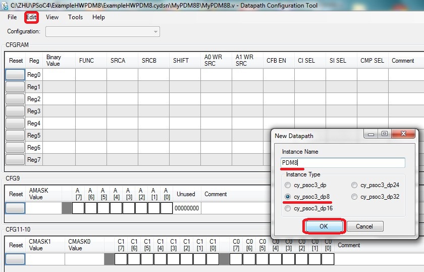
图6A
(6B)填写表格:我们只须把CFGRAM – Reg0的FUNC设为“ADD”,以及将ALU结果写回A0(A0 WR SRC 设为 ALU)就可以了,其余都与Default的设置一致,无需改动。(图6B)
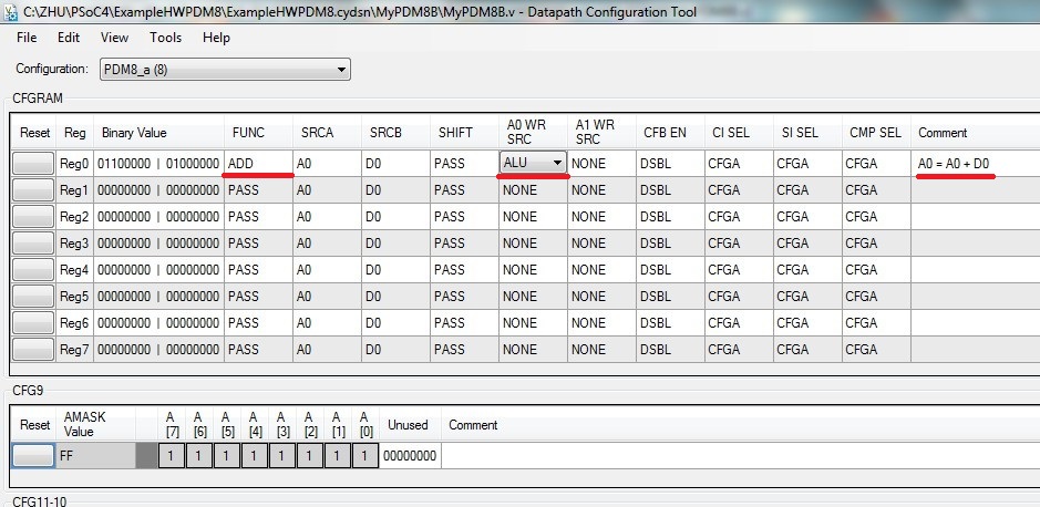
图6B
File – Save会自动写入MyPDM8B.v。然后File – Exit退出Tool环境,回到开发环境。这时开发环境主窗口中的MyPDM8B.v已加入了Datapath Config Tool所添加的Datapath Config内容。(图6C)
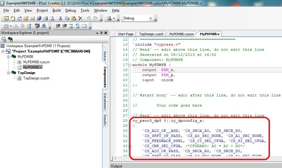
图6C
(7)人工编辑MyPDM8B.v。主要是连接Datapath的输入(将时钟clock连至clk)、输出(将加法的进位位co_msb输出至PDM_p及PDM_n);以及加一些注释。(图7A,图7B)。
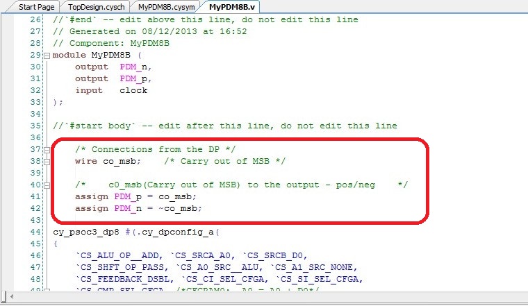
图7A
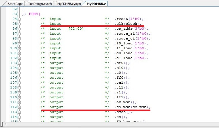
图7B
修改完成的MyPDM8B.v如下:
MyPDM8B.v
//`#start header` -- edit after this line, do not edit this line
// ========================================
//
// Copyright FY_ZHU, 2013
// All Rights Reserved
// UNPUBLISHED, LICENSED SOFTWARE.
//
// CONFIDENTIAL AND PROPRIETARY INFORMATION
// WHICH IS THE PROPERTY OF FY_ZHU.
//
// *The PDM Algorithm Based On Addition :
// *	 CNT += H ;
// * if ( CNT >= N )
// *    { CNT %= N ;  Pout = 1 ; }
// * else Pout = 0 ;
// *This algorithm generates H active output pulses in period N .
// *
// *The algorithm is free for all under mentioning that the algorithm is from author FY_ZHU.
// *
// *In this example the algorithm is implemented using hardware and software respectively.
// *Here the PDM output is generated by hardware, a datapath with only one operation : A0 = A0 + D0 .
//
// ========================================
`include "cypress.v"
//`#end` -- edit above this line, do not edit this line
// Generated on 08/12/2013 at 16:52
// Component: MyPDM8B
module MyPDM8B (
	output  PDM_n,
	output  PDM_p,
	input   clock
);

//`#start body` -- edit after this line, do not edit this line

	/* Connections from the DP */
	wire co_msb;	/* Carry out of MSB */

	/*    c0_msb(Carry out of MSB) to the output - pos/neg    */
	assign PDM_p = co_msb;
	assign PDM_n = ~co_msb;

cy_psoc3_dp8 #(.cy_dpconfig_a(
{
    `CS_ALU_OP__ADD, `CS_SRCA_A0, `CS_SRCB_D0,
    `CS_SHFT_OP_PASS, `CS_A0_SRC__ALU, `CS_A1_SRC_NONE,
    `CS_FEEDBACK_DSBL, `CS_CI_SEL_CFGA, `CS_SI_SEL_CFGA,
    `CS_CMP_SEL_CFGA, /*CFGRAM0:  A0 = A0 + D0*/
    `CS_ALU_OP_PASS, `CS_SRCA_A0, `CS_SRCB_D0,
    `CS_SHFT_OP_PASS, `CS_A0_SRC_NONE, `CS_A1_SRC_NONE,
    `CS_FEEDBACK_DSBL, `CS_CI_SEL_CFGA, `CS_SI_SEL_CFGA,
    `CS_CMP_SEL_CFGA, /*CFGRAM1:  */
    `CS_ALU_OP_PASS, `CS_SRCA_A0, `CS_SRCB_D0,
    `CS_SHFT_OP_PASS, `CS_A0_SRC_NONE, `CS_A1_SRC_NONE,
    `CS_FEEDBACK_DSBL, `CS_CI_SEL_CFGA, `CS_SI_SEL_CFGA,
    `CS_CMP_SEL_CFGA, /*CFGRAM2:  */
    `CS_ALU_OP_PASS, `CS_SRCA_A0, `CS_SRCB_D0,
    `CS_SHFT_OP_PASS, `CS_A0_SRC_NONE, `CS_A1_SRC_NONE,
    `CS_FEEDBACK_DSBL, `CS_CI_SEL_CFGA, `CS_SI_SEL_CFGA,
    `CS_CMP_SEL_CFGA, /*CFGRAM3:  */
    `CS_ALU_OP_PASS, `CS_SRCA_A0, `CS_SRCB_D0,
    `CS_SHFT_OP_PASS, `CS_A0_SRC_NONE, `CS_A1_SRC_NONE,
    `CS_FEEDBACK_DSBL, `CS_CI_SEL_CFGA, `CS_SI_SEL_CFGA,
    `CS_CMP_SEL_CFGA, /*CFGRAM4:  */
    `CS_ALU_OP_PASS, `CS_SRCA_A0, `CS_SRCB_D0,
    `CS_SHFT_OP_PASS, `CS_A0_SRC_NONE, `CS_A1_SRC_NONE,
    `CS_FEEDBACK_DSBL, `CS_CI_SEL_CFGA, `CS_SI_SEL_CFGA,
    `CS_CMP_SEL_CFGA, /*CFGRAM5:  */
    `CS_ALU_OP_PASS, `CS_SRCA_A0, `CS_SRCB_D0,
    `CS_SHFT_OP_PASS, `CS_A0_SRC_NONE, `CS_A1_SRC_NONE,
    `CS_FEEDBACK_DSBL, `CS_CI_SEL_CFGA, `CS_SI_SEL_CFGA,
    `CS_CMP_SEL_CFGA, /*CFGRAM6:  */
    `CS_ALU_OP_PASS, `CS_SRCA_A0, `CS_SRCB_D0,
    `CS_SHFT_OP_PASS, `CS_A0_SRC_NONE, `CS_A1_SRC_NONE,
    `CS_FEEDBACK_DSBL, `CS_CI_SEL_CFGA, `CS_SI_SEL_CFGA,
    `CS_CMP_SEL_CFGA, /*CFGRAM7:  */
    8'hFF, 8'h00,  /*CFG9:  */
    8'hFF, 8'hFF,  /*CFG11-10:  */
    `SC_CMPB_A1_D1, `SC_CMPA_A1_D1, `SC_CI_B_ARITH,
    `SC_CI_A_ARITH, `SC_C1_MASK_DSBL, `SC_C0_MASK_DSBL,
    `SC_A_MASK_DSBL, `SC_DEF_SI_0, `SC_SI_B_DEFSI,
    `SC_SI_A_DEFSI, /*CFG13-12:  */
    `SC_A0_SRC_ACC, `SC_SHIFT_SL, 1'h0,
    1'h0, `SC_FIFO1_BUS, `SC_FIFO0_BUS,
    `SC_MSB_DSBL, `SC_MSB_BIT0, `SC_MSB_NOCHN,
    `SC_FB_NOCHN, `SC_CMP1_NOCHN,
    `SC_CMP0_NOCHN, /*CFG15-14:  */
    10'h00, `SC_FIFO_CLK__DP,`SC_FIFO_CAP_AX,
    `SC_FIFO_LEVEL,`SC_FIFO__SYNC,`SC_EXTCRC_DSBL,
    `SC_WRK16CAT_DSBL /*CFG17-16:  */
}
)) PDM8(
        /*  input                   */  .reset(1'b0),
        /*  input                   */  .clk(clock),
        /*  input   [02:00]         */  .cs_addr(3'b0),
        /*  input                   */  .route_si(1'b0),
        /*  input                   */  .route_ci(1'b0),
        /*  input                   */  .f0_load(1'b0),
        /*  input                   */  .f1_load(1'b0),
        /*  input                   */  .d0_load(1'b0),
        /*  input                   */  .d1_load(1'b0),
        /*  output                  */  .ce0(),
        /*  output                  */  .cl0(),
        /*  output                  */  .z0(),
        /*  output                  */  .ff0(),
        /*  output                  */  .ce1(),
        /*  output                  */  .cl1(),
        /*  output                  */  .z1(),
        /*  output                  */  .ff1(),
        /*  output                  */  .ov_msb(),
        /*  output                  */  .co_msb(co_msb),
        /*  output                  */  .cmsb(),
        /*  output                  */  .so(),
        /*  output                  */  .f0_bus_stat(),
        /*  output                  */  .f0_blk_stat(),
        /*  output                  */  .f1_bus_stat(),
        /*  output                  */  .f1_blk_stat()
);
//`#end` -- edit above this line, do not edit this line
endmodule
//`#start footer` -- edit after this line, do not edit this line

//`#end` -- edit above this line, do not edit this line
至此,8位PDM部件MyPDM8B已经完成。就如PSoC Creator的其他部件一样,可以在开发环境中使用了。
例如,我们可以回到TopDesign的线路设计,在Default Component Catalog中找到MyPDM8B部件,把它拖放到设计图中。两个部件自动被命名为MyPDM8B_1、MyPDM8B_2(图8)。
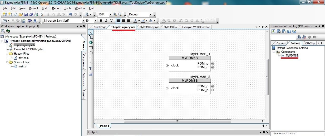
图8
在程序中,只须按需对Datapath中的D0寄存器赋值就可以了。
例如
/* Feed datapath with new value */
CY_SET_REG8(MyPDM8B_1_PDM8_u0__D0_REG, new_value); // 0~255
具体可参见文(1)中的实例。
上面仅介绍8位硬件PDM的做法,而16位硬件PDM的做法可依此类推。
PSoC4只有4块UDB,只可做4个8位硬件PDM,或2个16位硬件PDM。而PSoC3及PSoC5有有24块UDB,灵活性就大了。
How to Realize the Hardware PDM with PSoC UDB
- A PDM Algorithm Based On Addition (4)
===
FY_ZHU
2013-08-15 BOS-MA
基于累加的PDM算法(1) - 只用一条加法指令实现的PWM算法,软硬都行
基于累加的PDM算法(2) - 基于累加的PDM算法的原理
基于累加的PDM算法(3) - 硬件PWM与基于累加的硬件PDM的比较

