适合于PM-QPSK和PM-16QAM的相干光通信频偏估计和补偿算法IP核
0赞公司研制的基于A10 FPGA实现的频偏估计和补偿算法,消耗逻辑资源7.9K逻辑、14.9K分布式RAM资源、0乘法器,具有逻辑资源消耗小的优势,补偿频偏范围大,捕获频偏范围为+/-Baud/8,支持内核时钟速率440MHz,支持PM-QPSK/PM-16QAM/SP-QPSK/SP-16QAM等,支持波特率大于2.5Gaud。
该算法基于“Carrier Recovery for Satellite-to-ground Coherent Laser Communication Systems Using Double Feedback Loop and Viterbi-Viterbi Feedforward Cascade Structure”论文频偏估计和补偿算法实现,在星地相干光通信系统中,多普勒频移、收发信机激光频偏和基于扰动的激光稳频技术引起的高动态宽范围频偏是与地面光纤相干传输的重要区别之一。设计一种可靠的频偏捕获和精细载波跟踪算法对地面光学站至关重要。我们提出了两级反馈环和Viterbi-Viterbi(V-V)前馈级联载波恢复算法。第一阶段采用基于预判决的角度差分估计器(PADE)作为剩余频偏(RFO)估计器,以估计高动态、宽范围的频偏。然后在第二级中采用基于V-V的RFO估计器来精确地补偿剩余频率。V-V算法用于补偿相位偏移,与基于V-V的RFO估计器共享相同的逻辑资源。基于FPGA进行了10Gbps数据速率PM-QPSK实时实验,对算法性能进行了评估。所提出的级联算法在FOE的动态跟踪速度和归一化均方误差(MSE)方面表现出优异的性能。
1. 基于FPGA的实时实验设置

Fig. 2. Real-time experimental setup of the 10-Gbps data rate PM-QPSK modulation system and the DSP algorithms implemented in Arria® 10 FPGA. LD: Laser Diode, ABC: automatic bias controller, ATT: attenuator, EDFA: erbium doped fiber amplifier, ICR: integrated coherent receiver, LO: local oscillator.
The proposed carrier recovery algorithm is adopted in a 10-Gbps data rate PM-QPSK transceiver prototype developed by our research group, and the experimental setup is shown in Fig. 2. Transmitter hardware includes PM-QPSK electrical signal generation circuit based on FPGA (10ax066k3f40), four-channel microwave amplifier, automatic bias controller, laser (TTX1995) and optical PM-IQ modulator (FTM7977). The laser wavelength and linewidth are 1550.32 nm and 20 KHz, respectively. The optical signal with launch power of -3 dBm is obtained after PM-IQ modulator. The transmitter DSP algorithm implemented in FPGA includes RS (255, 239) coding, symbol mapping, etc. An optical attenuator before EDFA is used to adjust the received power. The electrical waveform after ICR is captured by ADC with sampling rate and resolution of 5 GSa/s and 8 bits, respectively. DSP demodulation algorithms are implemented in FPGA (10ax066k3f40), and its DSP core is driven by 312.5-MHz rate clock. I/Q imbalance compensation algorithm adopts the cascaded phase and gain imbalance scheme proposed and verified in our previous work [15]. The clock recovery is realized based on feedback structure that use Gardner timing error detector. 4×4 real-valued multiple-input multiple-output adaptive equalizer based on 3-taps is used to realize polarization demultiplexing and linear channel equalization [16]. Two samples per symbol and 16 parallel units (PUs) are performed in Cartesian coordinate before 4×4 real-valued MIMO, and single sample per symbol and 8 PUs are used in Polar coordinates after MIMO. Circuits developed by our research group used in this work are shown in the figure above, i.e. (i) PM-QPSK electrical signal generator, (ii) automatic bias controller, (iii) microwave amplifier, (iv) ICR driver, (v) four-channel ADCs and FPGA processing board. There is no hardware-implemented coarse FOE algorithm at present stage, thus manually adjust the RFO of the transceiver laser to be less than 300 MHz to meet the capture requirement of double feedback FOE.
2.基于FPGA的频偏估计性能分析

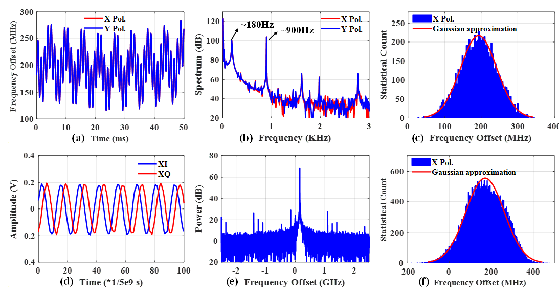
Fig. 3 (a) The measured FO of X and Y Pol. within 50 ms by using first-stage feedback FOE. (b) Spectrum analysis of FO variation. (c) The measured FO statistical count with statistical time of 120 seconds. (d) Time-domain and (e) frequency-domain diagrams of transceiver FO measured by beat frequency method. (c) The measured FO statistical count with statistical time of 6 hours.

Fig. 5. The measured FO by reading register ![]() at the first-stage feedback loop shown by blue line, and the measured actual FO shown by red line at the received power of (a) -45.5 dBm and (c) -47 dBm. The residual phase calculated in V-V algorithm versus time at the received power of (b) -45.5 dBm and (d) -47 dBm.
at the first-stage feedback loop shown by blue line, and the measured actual FO shown by red line at the received power of (a) -45.5 dBm and (c) -47 dBm. The residual phase calculated in V-V algorithm versus time at the received power of (b) -45.5 dBm and (d) -47 dBm.

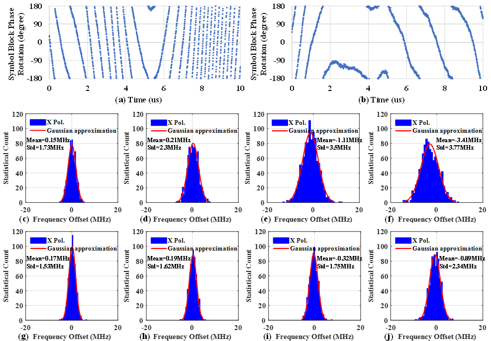
Fig. 6. The symbol block phase rotation calculated by FPGA-based V-V algorithm with (a) single feedback loop FOE and (b) double feedback loop FOE. The residual frequency offset statistical count with single feedback FOE at BER of (c) 1×10⁻⁴, (d) 1×10⁻³, (e) 3.8×10⁻³ and (f) 1×10⁻². The residual frequency offset statistical count with double feedback FOE at BER of (g) 1×10⁻⁴, (h) 1×10⁻³, (i) 3.8×10⁻³ and (j) 1×10⁻².

Fig. 7. (a) The effect of frequency offset on receiver sensitivity penalty with double feedback loop and V-V feedforward cascaded carrier recovery algorithm. (b) BER as a function of the received power at B2B processed by single-stage feedback FOE in FPGA, two-stage feedback FOE in FPGA, and two-stage feedback FOE in MATLAB®.
FPGA Logic Resource Consumption
Table 1. 10-Gbps data rate Coherent DSP algorithm logic resource consumption in Arria® 10 FPGA
Algorithm | ALMs (K) | Logic Register (K) | Hardware Multiplier |
I/Q imbalance compensation | 1.3 | 2.3 | 64 |
Gardner based clock recovery | 7.2 | 20.3 | 74 |
4×4 real-valued MIMO | 6.1 | 21.3 | 442 |
First-stage feedback FOE | 7.9 | 14.9 | 0 |
Second-stage feedback FOE | 1.2 | 3.2 | 0 |
V-V phase offset compensation | 1.4 | 5.2 | 0 |
RS(255,239) decoder | 2.2 | 4.1 | 0 |
Total consumption | 27.3 | 71.3 | 580 |

Fig. 8 (a) Experimental setup of feedforward and single-stage feedback FOEs in real-time FPGA processing. Frequency offset calculation position with (i) feedforward and (ii) feedback FOE. (b) The measured frequency offset curves of X and Y Pol. by employing feedforward and feedback FOEs at received power of -42.2 dBm.
